

�ЈD�W(w��ng)С����
һ�I���
������


>
>>
��(sh��)��ϵ�y(t��ng)�O(sh��)Ӌ(j��):Verilog �� VHDL��:Ӣ�İ�
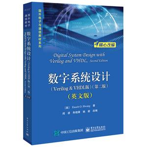
���] ��(sh��)��ϵ�y(t��ng)�O(sh��)Ӌ(j��):Verilog �� VHDL��:Ӣ�İ�
�_(k��i)����
26cm
�(y��)��(sh��)��
14,405
���Σ��̲��N����
¥25.6(3.2��)?
�A(y��)�����փr(ji��)�ǰ����c���N���(d��ng)�����(y��u)�ݵ�ُ(g��u)�I����Ӌ(j��)����ăr(ji��)������(y��u)��ȯ���֣����H��������δ�ص�ͬ�ڌ�(sh��)�H���փr(ji��)��
00:00:00
���N���(d��ng):
��ܰ��ʾ��5�����D����Ҫ�������β؛���֞�ȫ�£����ܷ�/�o(w��)�ܷ⣩����(g��)�e�D��Ʒ��8-9���¡��п�
�Є�����(bi��o)ӛ����P�ȸ�����ȫԔ��(x��)Ʒ���f(shu��)��>>
�Є�����(bi��o)ӛ����P�ȸ�����ȫԔ��(x��)Ʒ���f(shu��)��>>
������Ǖ�����>
-
>
�J�M(j��n)��(sh��)�W(xu��)����D�D̽�ؚvʷ���}

-
>
���t(y��)���A(ch��)��Փ
-
>
��(d��ng)���Ї�(gu��)�����c����(�¾�21���o(j��)��������ϵ�н̲�)
-
>
��У܊���n�̳�
-
>
˼������c����(2021���)
-
>
ë�ɖ|˼����Ї�(gu��)��ɫ���(hu��)���x��Փ�wϵ��Փ(2021���)
-
>
���t(y��)��(n��i)�ƌW(xu��)��ȫ��(gu��)���t(y��)ˎ�ИI(y��)�ߵȽ�����ʮ���塱Ҏ(gu��)���̲�

�������đ�(zh��n)��(ch��ng)���P(gu��n)����؛���c�Q(m��o)��](http://image31.bookschina.com/pro-images/250513gs/487100.jpg?id=81)
�ЈD�r(ji��):¥42.7
����ُ(g��u)��܇
��(sh��)��ϵ�y(t��ng)�O(sh��)Ӌ(j��):Verilog �� VHDL��:Ӣ�İ� ���(qu��n)��Ϣ
- ISBN��9787121334214
- �l�δa��9787121334214 ; 978-7-121-33421-4
- �b����һ���z�漈
- ��(c��)��(sh��)�����o(w��)
- ���������o(w��)
- ���ٷ��>>
��(sh��)��ϵ�y(t��ng)�O(sh��)Ӌ(j��):Verilog �� VHDL��:Ӣ�İ� ������ɫ
�S����Ӽ��g(sh��)�cӋ(j��)��C(j��)���g(sh��)���w�ٰl(f��)չ���Լ����M(j��n)������O(sh��)Ӌ(j��)�Ԅ�(d��ng)����EDA�����g(sh��)���F(xi��n)��(ch��ng)�ɾ����T��У�FPGA�������ďV����(y��ng)�ã��F(xi��n)����(sh��)��߉�·�cϵ�y(t��ng)���O(sh��)Ӌ(j��)�����(sh��)�F(xi��n)���g(sh��)�ѽ�(j��ng)�l(f��)���˷��츲�ص�׃����������̎����ϵ�y(t��ng)�����(f��)�s��(sh��)��߉ϵ�y(t��ng)�Ĵ������ں�(ji��n)Ҫ��B�乤��ԭ���Ļ��A(ch��)�ϣ���CPUӲ���Y(ji��)��(g��u)��D�龀��؞������(g��)�¹�(ji��)��Ԕ��(x��)�v������Θ�(g��u)�������M��/�r(sh��)��߉Ԫ���������������Ԫ���M����(sh��)��(j��)ͨ·�c���Ɔ�Ԫ����������������в�����(sh��)�F(xi��n)һ��(g��)ͨ��CPU���Լ����ͨ�^(gu��)�M(j��n)һ�����Ӻ�(ji��n)�ε�ݔ��ݔ���ӿځ�(l��i)*�K���һ��(g��)������̎����ϵ�y(t��ng)������ͨ�^(gu��)�ں�(ji��n)�εĔ�(sh��)��߉Ԫ���c��(f��)�s�Č�(sh��)�Ô�(sh��)��߉ϵ�y(t��ng)֮�g��������܉�����x��������┵(sh��)��߉�M�����O(sh��)Ӌ(j��)�cʹ�÷������M(j��n)��ȫ��������ذ��Տ�(f��)�s��(sh��)��ϵ�y(t��ng)��EDA�O(sh��)Ӌ(j��)�c��(sh��)�F(xi��n)���g(sh��)Ҫ�c(di��n)�����������P(gu��n)�W(w��ng)վ�ṩ���S���Č�(sh��)�ÌW(xu��)��(x��)�YԴ�������O(sh��)Ӌ(j��)ʾ�����ṩ���·�D�Լ�Verilog�cVHDLԴ�a��
��(sh��)��ϵ�y(t��ng)�O(sh��)Ӌ(j��):Verilog �� VHDL��:Ӣ�İ� ��(n��i)�ݺ�(ji��n)��
����ͨ�^(gu��)�ں�(ji��n)�εĔ�(sh��)��߉Ԫ���c��(f��)�s�Č�(sh��)�Ô�(sh��)��߉ϵ�y(t��ng)֮�g��������܉�����x��������┵(sh��)��߉�M�����O(sh��)Ӌ(j��)�cʹ�÷������M(j��n)��ȫ��������ذ��Տ�(f��)�s��(sh��)��ϵ�y(t��ng)��EDA�O(sh��)Ӌ(j��)�c��(sh��)�F(xi��n)���g(sh��)Ҫ�c(di��n)�����������P(gu��n)�W(w��ng)վ�ṩ���S���Č�(sh��)�ÌW(xu��)��(x��)�YԴ�������O(sh��)Ӌ(j��)ʾ�����ṩ���·�D�Լ�Verilog�cVHDLԴ�a��
��(sh��)��ϵ�y(t��ng)�O(sh��)Ӌ(j��):Verilog �� VHDL��:Ӣ�İ� Ŀ�
Chapter 1��Introduction to Microprocessor Design
1.1��Overview of Microprocessor Design
1.2��Design Abstraction Levels
1.3��Examples of a 2-to-1 Multiplexer
1.3.1��Behavioral Level
1.3.2��Gate Level
1.3.3��Transistor Level
1.4��Introduction to Hardware Description Language
1.5��Synthesis
1.6��Going Forward
1.7��Problems
Chapter 2��Fundamentals of Digital Circuits
2.1��Binary Numbers
2.1.1��Counting in Binary
2.1.2��Converting between Binary and Decimal
2.1.3��Octal and Hexadecimal Notations
2.1.4��Binary Number Arithmetic
2.2��Negative Numbers
2.2.1��Two’s Complement Representation
2.2.2��Sign Extension
2.2.3��Signed Number Arithmetic
2.3��Binary Switch
2.4��Basic Logic Operators and Logic Expressions
2.5��Logic Gates
2.6��Truth Tables
2.7��Boolean Algebra and Boolean Equations
2.7.1��Boolean Algebra
2.7.2��Duality Principle
2.7.3��Boolean Functions and Their Inverses
2.8��Minterms and Maxterms
2.8.1��Minterms
2.8.2��Maxterms
2.9��Canonical, Standard, and Non-Standard Forms
2.10��Digital Circuits
2.11��Designing a Car Security System
2.12��Verilog and VHDL Code for Digital Circuits
2.12.1��Verilog Code for a Boolean Function
2.12.2��VHDL Code for a Boolean Function
2.13��Problems
Chapter 3��Combinational Circuits 65
3.1��Analysis of Combinational Circuits
3.1.1��Using a Truth Table
3.1.2��Using a Boolean Function
3.2��Synthesis of Combinational Circuits
3.2.1��Using Only NAND Gates
3.3��Minimization of Combinational Circuits
3.3.1��Boolean Algebra
3.3.2��Karnaugh Maps
3.3.3��Don’t-Cares
3.3.4��Tabulation Method
3.4��Timing Hazards and Glitches
3.4.1��Using Glitches
3.5��BCD to 7-Segment Decoder
3.6��Verilog and VHDL Code for Combinational Circuits
3.6.1��Structural Verilog Code
3.6.2��Structural VHDL Code
3.6.3��Dataflow Verilog Code
3.6.4��Dataflow VHDL Code
3.6.5��Behavioral Verilog Code
3.6.6��Behavioral VHDL Code
3.7��Problems
Chapter 4��Standard Combinational Components
4.1��Signal Naming Conventions
4.2��Multiplexer
4.3��Adder
4.3.1��Full Adder
4.3.2��Ripple-Carry Adder
4.3.3��Carry-Lookahead Adder
4.4��Subtractor
4.5��Adder-Subtractor Combination
4.6��Arithmetic Logic Unit
4.7��Decoder
4.8��Tri-State Buffer
4.9��Comparator
4.10��Shifter
4.11��Multiplier
4.12��Problems
Chapter 5 Sequential Circuits
5.1��Bistable Element
5.2��SR Latch
5.3��Car Security System—Version 2
5.4��SR Latch with Enable
5.5��D Latch
5.6��D Latch with Enable
5.7��Verilog and VHDL Code for Memory Elements
5.7.1��VHDL Code for a D Latch with Enable
5.7.2��Verilog Code for a D Latch with Enable
5.8��Clock
5.9��D Flip-Flop
5.9.1��Alternative Smaller Circuit
5.10��D Flip-Flop with Enable
5.10.1��Asynchronous Inputs
5.11��Description of a Flip-Flop
5.11.1��Characteristic Table
5.11.2��Characteristic Equation
5.11.3��State Diagram
5.12��Register
5.13��Register File
5.14��Memories
5.14.1��ROM
5.14.2��RAM
5.15��Shift Registers
5.15.1��Serial-to-Parallel Shift Register
5.15.2��Serial-to-Parallel and Parallel-to-Serial Shift Register
5.15.3��Linear Feedback Shift Register
5.16��Counters
5.16.1��Binary Up Counter
5.16.2��Binary Up Counter with Parallel Load
5.17��Timing Issues
5.18��Problems
Chapter 6��Finite-State Machines
6.1��Finite-State Machine Models
6.2��State Diagrams
6.3��Analysis of Finite-State Machines
6.3.1��Next-State Equations
6.3.2��Next-State Table
6.3.3��Output Equations
6.3.4��Output Table
6.3.5��State Diagram
6.3.6��Example
6.4��Synthesis of Finite-State Machines
6.4.1��State Diagram
6.4.2��Next-State Table
6.4.3��Next-State Equations
6.4.4��Output Table and Output Equations
6.4.5��FSM Circuit
6.5��Optimizations for FSMs
6.5.1��State Reduction
6.5.2��State Encoding
6.5.3��Unused States
6.6��FSM Construction Examples
6.6.1��Car Security System—Version 3
6.6.2��Modulo-6 Up-Counter
6.6.3��One-Shot Circuit
6.6.4��Simple Microprocessor Control Unit
6.6.5��Elevator Controller Using a Moore FSM
6.6.6��Elevator Controller Using a Mealy FSM
6.7��Verilog and VHDL Code for FSM Circuits
6.7.1��Behavioral Verilog Code for a Moore FSM
6.7.2��Behavioral Verilog Code for a Mealy FSM
6.7.3��Behavioral VHDL Code for a Moore FSM
6.7.4��Behavioral VHDL Code for a Mealy FSM
6.8��Problems
Chapter 7��Dedicated Microprocessors
7.1��Need for a Datapath
7.2��Constructing the Datapath
7.2.1��Selecting Registers
7.2.2��Selecting Functional Units
7.2.3��Data Transfer Methods
7.2.4��Generating Status Signals
7.3��Constructing the Control Unit
7.3.1��Deriving the Control Signals
7.3.2��Deriving the State Diagram
7.3.3��Timing Issues
7.3.4��Deriving the FSM Circuit
7.4��Constructing the Complete Microprocessor
7.5��Dedicated Microprocessor Construction Examples
7.5.1��Greatest Common Divisor
7.5.2��High-Low Number Guessing Game
7.5.3��Traffic Light Controller
7.6��Verilog and VHDL Code for Dedicated Microprocessors
7.6.1��FSM1D Model
7.6.2��FSMD Model
7.6.3��Algorithmic Model
7.7��Problems
Chapter 8��General-Purpose Microprocessors
8.1��Overview of the CPU Design
8.2��The EC-1 General-Purpose Microprocessor
8.2.1��Instruction Set
8.2.2��Datapath
8.2.3��Control Unit
8.2.4��Complete Circuit
8.2.5��Sample Program
8.2.6��Simulation
8.2.7��Hardware Implementation
8.3��The EC-2 General-Purpose Microprocessor
8.3.1��Instruction Set
8.3.2��Datapath
8.3.3��Control Unit
8.3.4��Complete Circuit
8.3.5��Sample Program
8.3.6��Hardware Implementation
8.4��Extending the EC-2 Instruction Set
Chapter 9��Interfacing Microprocessors
9.1��Multiplexing 7-Segment LED Display
9.1.1��Theory of Operation
9.1.2��Controller Design
9.2��Issues with Interfacing Switches
9.3��3×4 Keypad Controller
9.3.1��Theory of Operation
9.3.2��Controller Design
չ�_(k��i)ȫ��
��(sh��)��ϵ�y(t��ng)�O(sh��)Ӌ(j��):Verilog �� VHDL��:Ӣ�İ� ���ߺ�(ji��n)��
Enoch O. Hwang ������(gu��)���ݴ�W(xu��)Riverside��У�@Ӌ(j��)��C(j��)�ƌW(xu��)��ʿ�W(xu��)λ��Ŀǰ���ϼ���Sierra��W(xu��)Ӌ(j��)��C(j��)�ƌW(xu��)ϵ�������ڣ����ݴ�W(xu��)Riverside��У��ӹ���ϵ��Ӌ(j��)��C(j��)�ƌW(xu��)�c����ϵ�v������Ҫ�v�ڔ�(sh��)��߉�O(sh��)Ӌ(j��)�n�̡�
Enoch O. Hwang ������(gu��)���ݴ�W(xu��)Riverside��У�@Ӌ(j��)��C(j��)�ƌW(xu��)��ʿ�W(xu��)λ��Ŀǰ���ϼ���Sierra��W(xu��)Ӌ(j��)��C(j��)�ƌW(xu��)ϵ�������ڣ����ݴ�W(xu��)Riverside��У��ӹ���ϵ��Ӌ(j��)��C(j��)�ƌW(xu��)�c����ϵ�v������Ҫ�v�ڔ�(sh��)��߉�O(sh��)Ӌ(j��)�n�̡�
�������]
- >
����Ԣ��-�����ČW(xu��)�������-ȫ�g��
- >
��(j��ng)�䳣Մ
- >
����?gu��)����x��Ѹ:�����¾�
- >
������x�c�ղء������ČW(xu��)����:һ��Ĺ���
- >
�����������
- >
���c�؉�
- >
������
- >
����c�ƴ��Ļ�
����N