

�ЈD�W(w��ng)С����
һ�I���
������


>
>>
��(sh��)��VLSIоƬ�O(sh��)Ӌ(j��)-ʹ��Cadence��Synopsys CAD����
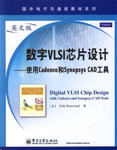
���] ��(sh��)��VLSIоƬ�O(sh��)Ӌ(j��)-ʹ��Cadence��Synopsys CAD����
���م�����
��(gu��)������cͨ�Ž̲�ϵ��
�_����
16�_
퓔�(sh��)��
571
������Ǖ�����>
-
>
��·܇����(ZINN�Ĺ�·܇�S���c���B(y��ng)�ؼ�)

-
>
���w���·�O(sh��)Ӌ(j��)(��)
-
>
���ڂ�(g��)�Ի��O(sh��)Ӌ(j��)���Ե����ܽ�ͨϵ�y(t��ng)�P(gu��n)�I���g(sh��)
-
>
���Ӱٳ�:�F���ٔ�(sh��)����D����ɫ
-
>
ɽ�|��������������˾���g(sh��)�D(zhu��n)���c���g(sh��)��(chu��ng)�vʷ�����Ї�(gu��)�ߵȼ��g(sh��)�������K��(1949��1961)�Ա����^(q��)������
-
>
�F·�C(j��)܇��Ҫ.��������(d��ng)��(n��i)ȼ.����C(j��)܇
-
>
���S̹�ĵ�������:���ڬF(xi��n)�������܌W(xu��)�Ć��}�c�}�j(lu��)
�ЈD�r(ji��):¥44.2
���r(sh��)ȱ؛

![�]�������đ�(zh��n)��(ch��ng)���P(gu��n)����؛���c�Q(m��o)��](http://image31.bookschina.com/pro-images/250513gs/487100.jpg?id=81)
��(sh��)��VLSIоƬ�O(sh��)Ӌ(j��)-ʹ��Cadence��Synopsys CAD���� ���(qu��n)��Ϣ
- ISBN��9787121091599
- �l�δa��9787121091599 ; 978-7-121-09159-9
- �b�������o
- ��(c��)��(sh��)�����o
- ���������o
- ���ٷ��>>
��(sh��)��VLSIоƬ�O(sh��)Ӌ(j��)-ʹ��Cadence��Synopsys CAD���� ��(n��i)�ݺ�(ji��n)��
������B���ʹ��cadence��synopsys��˾��cad���߁팍(sh��)�H�O(sh��)Ӌ(j��)��(sh��)��vlsiоƬ���x��ͨ�^��������ѭ��u�M(j��n)�،W(xu��)��(x��)�@Щcad���ߣ���ʹ���@Щܛ���O(sh��)Ӌ(j��)��������Ĕ�(sh��)�ּ����·оƬ��������(n��i)�ݰ������·���O(sh��)Ӌ(j��)���̾��ţ�����cad�O(sh��)Ӌ(j��)ƽ�_(t��i)���·�Dݔ�롢verilog���桢��D������(bi��o)��(zh��n)��Ԫ�O(sh��)Ӌ(j��)��ģ�M�͔�(sh��)ģ�����̖(h��o)���桢��Ԫ�����ͽ��졢verilog�C�ϡ�������ʽ���ɡ����ֲ�����оƬ���ɵȹ��ߣ�ÿһ���ߵ�ʹ�ö��Ԍ�(sh��)���f����*��o����һ��(g��)�O(sh��)Ӌ(j��)��(ji��n)��mips̎�������������ӡ��������c���P(gu��n)�����·�O(sh��)Ӌ(j��)��Փ�Ľ̿ƕ�����ʹ�ã�������ߵ�ԺУ���P(gu��n)�����·�O(sh��)Ӌ(j��)��Փ��n�̵����̲ĺͼ����·�O(sh��)Ӌ(j��)��(sh��)�`��n�̵Ľ̿ƕ���Ҳ�����鼯���·�O(sh��)Ӌ(j��)�ˆT����Ӗ(x��n)�̲ĺ�ʹ���փ�(c��)��
��(sh��)��VLSIоƬ�O(sh��)Ӌ(j��)-ʹ��Cadence��Synopsys CAD���� Ŀ�
1��introduction
��1.1 cad tool flows
1.1.1 custom vlsi and cell design flow
1.1.2 hierarchical cell/block asic flow
1.2 what this book is and isn't
1.3 bugs in the tools?
1.4 tool setup and execution scripts
1.5 typographical conventions
2��cadence dfii and icfb
��2.1 cadence design framework
��2.2 starting cadence
��2.3 summary
3��composer schematic capture
��3.1 starting cadence and making a new
��working library
��3.2 creating a new cell
3.2.1 creating the schematic view of a full adder
3.2.2 creating the symbol view of a full adder
3.2.3 creating a two-bit adder using the fulladder bit
��3.3 schematics that use transistors
��3.4 printing schematics
3.4.1 modifying postscript plot files
3.5 variable, pin, and cell naming restrictions
3.6 summary
4 verilog simulation
4.1 verflog simulation of composer schematics
��4.1.1 verilog-xl: simulating a schematic
4.1.2 nc_verilog: simulating a schematic
4.2 behavioral verilog code in composer
4.2.1 generating a behavioral view
4.2.2 simulating a behavioral view
4.3 stand-alone verilog simulation
4.3.1 verilog-xl
4.3.2 nc_verilog
4.3.3 vcs
4.4 timing in verilog simulations
4.4l behavioral versus transistor switch simulation
4.4.2 behavioral gate timing
4.4.3 standard delay format (sdf) timing
4.4.4 transistor timing
��4.5 summary
5��virtuoso layout editor
5.1 an inverter schematic
��5.1.1 starting cadence kfb
5.1.2 making an inverter schematic
5.1.3 making an inverter symbol
5.2 layout for an inverter
5.2.1 creating a new layout view
5.2.2 drawing an nmostransistor
5.2.3 drawing a pmos transistor
5.2.4 assembling the inverter from the transistor layouts
5.2.5 using hierarchy in layout
5.2.6 virtuoso command overview
������
6 standard cell design template
7 spectre analog simulator
8 cell characterization
9 verilog synthesis
10 abstract generation
11 soc encounter place and route
12 chip assembly
13 design example
a tool and setup scripts
b scripts to drive the tools
c technology and cell libraries
bibliography
index
չ�_ȫ��
�������]
- >
�����S�����-�������Ծ���
- >
���������~����Փ/���С��
- >
������x�c�ղء������ČW(xu��)����:һ��Ĺ���
- >
����
- >
���c�؉�
- >
���Z�ڴ���ϵ�С������˼��20:Փ��Ȼ�x��(Ӣ�h�p�Z)
- >
���ČW(xu��)���ɾ���--��Ѹ�c���m/�t�T�W(xu��)�g(sh��)����(�t�T�W(xu��)�g(sh��)����)
- >
Ԋ��(j��ng)-����ĸ質
����N